An Introduction to HDI PCBs: What Every Electronics Manufacturer Should Know
HDI PCBs are among the most cherished products that are applied widely in the high-tech electronic field with the fast pace of development. This is so since as devices continue to be produced in smaller and multifaceted ways, the high-density interconnect PCBs offer the sort of versatility required to address these situations. Here is our brief on the HDI PCBs, and below are the factors that will be discussed about the electronics manufacturing companies.
Understanding HDI PCBs
The HDI PCBs have more interconnects as compared to the conventional PCB and they exhibit density in their interconnections. High-density manufacturing technologies employ microvias, blind vials, and buried vials to attain highly-density interconnect solutions in a confined space. The previous design is beneficial in that it offers higher circuit density and utility due to the reduction of the board and its weight.
Following are the few benefits of using High-Density Interconnect (HDI) PCBs:
Component Density is High: This depicts the more recent electronics integration PCB as the one that can accommodate more substantial elements within a relatively small area, which is the dream of many electronics product manufacturers in this age of shrinking electronics form factor for portability and compactness, especially in smart mobile devices such as smartphones, tablet PCs, and wearable electronics among others.
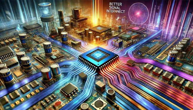
Better signal integrity: It is greatly preferable to have the signal paths as short as possible and the impedance of the HDI PCB to be low this enhances the signal integrity. The following are the advantages, wherein better performance and reliability will be represented particularly in handling high-speed as well as high-frequency applications.
Improved Thermal Management: HDI PCBs are conducive in as much as integration of thermal vias and heat sinks; thus, the board’s thermal management will be enhanced. This is good for high-power rating applications. This will avoid heating which if gets to a certain level will pose prospective issues.
Reduced Electromagnetic Interference: optimum design density and precise definition of the paths of the High-Density Interconnection PCB board help in controlling EMI, thus having a crucial role in ensuring signal integrity and, therefore, device performance.
Manufacturing Considerations
Design Complexity: HDI PCB design is complex and involves several activities that need extensive knowledge of advanced tools and methods.
Selection of Material: The choice of the material used to manufacture the HDI PCB has a significant impact on its performance. Plastics and other reinforcement substrates with good quality have to be selected to provide thermals and electricity in line with the HDI structures. Furthermore, appropriate material compatibility of the part considered must be considered with state-of-the-art manufacturing processes.
Cost Implications: Several benefits associated with HDI PCBs are that, they are realized from higher manufacturing processes and are even costlier than basic PCBs. The manufacturer has to strike a balance between the possibilities of enhancing performance and the idea of miniaturization to estimate the related costs. For all of this masks at an upstream level into product pricing and market strategy.
Manufacturing of PCBs for HDI: The production of HDI PCBs utilizes certain techniques namely microvias laser drilling, sequential laminations to develop the layers, and other alignment processes. Hence, the manufacturers have to make sure they have every requirement in terms of equipment and experience in using the enhanced processing techniques.
Applications of HDI PCBs
HDI PCBs are involved in various applications in the high-tech segment and this is so in those electronic consumer products like smartphones, tablets, laptops, and so on where space or performance may be a vital factor. In the automotive field, HDI technology enables the control units to integrate numerous complicated functions into the smallest chip area. Last but not least, consumer electronics equipment including medical devices and aerospace projects cannot do without high-density interconnect (HDI) PCBs due to reliability and precision.
Conclusion
Thus, it can be said, that by understanding and utilizing the potential of the HDI PCB technology, one will be able to highlight competitive advantages in the market of electronic manufacturers. Due to better density, improved signals, and efficient thermal dissipation, it is possible to develop complex but compact electronic products on the board from HDI PCBs. At the same time, manufacturers are necessitated to understand that the intricacies and expenses of the aforementioned technology cannot be optimally utilized in full measure. Thus, high-density interconnect or HDI PCBs will virtually remain indispensable in the manufacture of new and exciting electronic devices, as consumers’ preference for newer generations of ever-thinner and more powerful gadgetry grows by the day.